• TECH MANTRA

Enjoy a fast, responsive and cost effective Remote IT Support service to solve your IT issues quickly and with the minimum of fuss.Focused on building innovative solutions that create value for businesses and consumers. Our solutions are built around the following three founding principles - Unique Technology; Distinctive Information / Content; and Innovative Services. Our solutions combine these three, leverage our global services delivery capabilities and ensure that we are able to provide unmatched, superior resolution to specific customer problems.


Techmantra

Monday 6 April 2015

BIOS ALL THINGS NEED TO KNOW


BIOS stands for ,"Basic Input Output System". When a computer starts (power is first applied) there must be some program code which the CPU executes. This code executes before the operating system (Windows, Linux, etc.) loads. This code is contained in a memory chip(s) on the motherboard. When you start your computer anything you see on the screen before the operating system starts comes from code in the BIOS. This is why if a BIOS update fails or the BIOS becomes corrupt the computer appears to be dead; there is no code to execute. When BIOS code executes, it establishes a fixed software foundation which allows the operating system to link to the hardware on the motherboard. As CPUs and motherboard technology have become faster and more complex the size and speed of the memory chips required to store the BIOS code have also grown. What follows explains the history of BIOS chip evolution._______________________________________________________________________

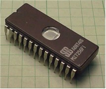
UV EPROMS - THE FIRST BIOS CHIPS


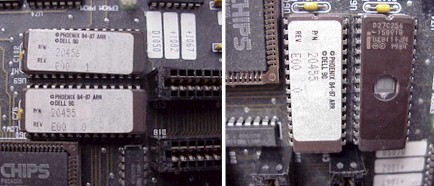
A UV EPROM (Ultraviolet Erasable) cannot be upgraded in the motherboard. The BIOS chip(s) must be removed, erased in an eprom eraser, and then reprogrammed with the updated code. Notice that there are two chips, this is because each chip is capable of delivering 8 bits of data. The early processors were 16 bits therefore you needed two 8 bit chips to deliver 16 bits in parallel. Also notice that on the label, in addition to the version information, there is a 0 and a 1. The 0 chip is the low order 8 bits and the 1 chip is the high order 8 bits. UV EPROM part numbers are 27 or 27C series (such as 27C256 or 27C512).
_______________________________________________________________________

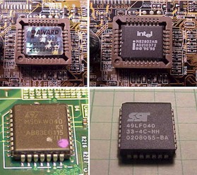
FLASH EPROMS - 2ND GENERATION BIOS CHIPS


The first BIOS chips, UV EPROMs, were fabricated in packages with pins on two sides. These were called "Dual In-line" or "DIP" as there were two rows of pins on each side of the package. This same package was also used for FLASH EPROMs as they allow easy socketing of the parts. As motherboard manufacturers added additional features and interfaces, board space became a limiting factor. To gain space the BIOS DIP package was abandoned in favor of the smaller PLCC or "Plastic Leaded Chip Carrier". The PLCC package has pins on four sides and is about the size of a postage stamp. In some cases the PLCC BIOS is soldered directly to the motherboard which makes reprogramming a failed part extremely difficult. The photo on the right shows the same FLASH part (A290021) in both a DIP and PLCC package. These parts are exactly the same except for the package._______________________________________________________________________

FIRMWARE HUBS - THE 3RD GENERATION OF BIOS


As technology progressed, more functionality became concentrated in the motherboard chip set. The chip set provides the link between the processor and the hardware subsystems on the motherboard including the BIOS which was fabricated in a combination I/O and memory part called a FIRMWARE HUB. When the computer starts the chip set reads the BIOS data from the FIRMWARE HUB and loads it into system RAM. The processor then executes the BIOS code from RAM instead of from the part itself. This is different from how the original BIOS chips worked and has paved the way for the current versions of BIOS chips. FIRMWARE HUB parts were initially released by INTEL as they were the primary supplier of motherboard processors. FIRMWARE HUB parts are usually fabricated in 32 PIN PLCC packages._______________________________________________________________________

HIGH-SPEED SERIAL SPI FLASH EPROMS - TODAYS BIOS TECHNOLOGY


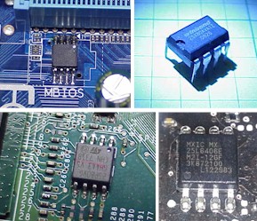
Modern motherboards, flat screen TVs, DVD players, home theatre receivers plus many other electronic products are now based on sophisticated, complex designs which start by booting from a BIOS chip. These products use the latest in high-speed, low cost memory technology parts called HI-SPEED SERIAL SPI FLASH EPROMs. SPI stands for "Serial Peripheral Interface". The SPI interface has existed for several decades but has now been incorporated into a flash eprom based high capacity part. The HI-SPEED SERIAL SPI FLASH EPROM is fabricated in either a DIP or surface mount 8 pin package. The SPI interface is serial (one bit at a time) which means that the data transfer speed must be extremely fast. As with a FIRMWARE HUB part, the SPI FLASH EPROMs function via the chip set to move the BIOS code from the part to system RAM for execution._______________________________________________________________________

FOR MORE INFORMATION CLICK THE LINKS BELOW


  • UPDATING BIOS (MOTHERBOARD BASED UTILITIES)
  • BIOS BEEP CODES
  • WHEN YOU SHOULD UPDATE YOUR BIOS


    NOTICE

    BIOS updates will not make your computer faster, they generally won’t add new features you need, and they may even cause additional problems. You should only update your BIOS if the new version contains an improvement you need.

    ________________________________________________________________

    KNOWLEDGE BASE


  • BIOS updates may be released to fix existing bugs, add support for new hardware and standards or add functionality. Read the release notes or other documentation for the BIOS update you're considering to see if the update will benefit your PC.

  • The BIOS provides an operating system with information about hardware, and is designed to support a specific range of components. The BIOS itself is typically an EEPROM, or Electronically Erasable Programmable Read-Only Memory, that is programmed with "firmware" and has the ability to save small amounts of information specific to user configurations. BIOS components are often soldered to the motherboard and therefore not serviceable by the user. Others can be inserted into a socket, making it easy to replace with a new one.

  • If the BIOS firmware has become corrupted and you have a similar motherboard with the same CPU socket and a BIOS chip of the same type, you may be able to recover your corrupt BIOS if you are willing to risk the other BIOS chip.

  • If your system is currently working well, perform a BIOS update only if you're willing to part with it (for an extended period of time) in the event of a critical failure. System builders and motherboard manufacturers will often repair systems and motherboards that failed to take a BIOS update, provided they are still under warranty.

  • ________________________________________________________________

    WARNINGS


  • Make sure to obtain the BIOS upgrade software from a reliable source. Downloading a BIOS from sources other than the manufacturer's web site is risky. For example, versions from the same BIOS software developer for one manufacturer's motherboard may not work on a different manufacturer's motherboard. Using the wrong BIOS or version might "brick" the board, thereby requiring either a BIOS replacement or reprogramming of the BIOS by the manufacturer and rendering the computer unable to boot until that is done.

  • The process itself is fragile since any power fluctuation during a flash may irrevocably corrupt the firmware. Great care needs to be taken in order to safely accomplish this.

  • Avoid updating the BIOS unless you know exactly what you are doing. Failure to follow a manufacturer's directions and precautions may corrupt the BIOS as well.

  • Make sure the electrical power source is reliable when flashing a BIOS. Any sizable fluctuation or loss of power during a flash process can corrupt the BIOS. Therefore, never power down or reset a PC when flashing the BIOS. If flashing the BIOS from a booted OS, first disable all unnecessary applications and background processes.

  • ________________________________________________________________

    DOWNLOADS


    ALL-IN-ONE UPDATE UTILITIES BASED ON MOTHERBOARD MANUFACTURERS

  • Download Gigabyte Bios update Utility (Universal Gigabyte Utility)

  • Download Intel Bios update Utility (Universal Intel Utility)

  • Download Asus Bios update Utility (Universal Asus Utility)

  • Download ECS Bios update Utility (Universal ECS Utility)

  • FLASHERS BASED ON BIOS CHIP MANUFACTURERS

  • AMI BIOS FLASH UTILITY

  • Thursday 2 April 2015

    Make Your own Printed Circuit Board (PCB)

    A printed circuit board (PCB) mechanically supports and electrically connects electronic components using conductive tracks, pads and other features etched from copper sheets laminated onto a non-conductive substrate. PCBs can be single sided (one copper layer), double sided (two copper layers) or multi-layer.

    Step 1: Print


    Once we design, we print each layer on a Propalcote paper (like the used to print the magazines) , to finalize the design know the dimensions so the plate will acquire a copper-clad board be a little larger than the dimensions of our design.

    Designing Softwares in common -Oracd,Eaglecad,SImplePcb etc.

    Step 2: Cleaning


    Once we have the copper-clad board is recommended to clean the grip toner, in this case, we clean with a sponge to wash the pots. After cleaning the copper-clad board is necessary to avoid contact our fingers with copper to prevent staining of fat, I recommend using latex gloves will be useful later.

    Step 3: Cut and paste


    At this point we turn to the scissors and tape, we will cut one of the prints. When we cut the print to leave some more paper for something like fins in combination with the tape can hold more paper to the copper-clad board.

    Step 4: Iron


    Now comes the part that usually make some mistakes, but with practice can be avoided. With the board we will transfer the toner to the copper-clad board with this protect our circuit tracks of acid attack. As I mentioned before this part is somewhat critical, because if you apply heat for a short time toner not going to be well attached to copper and if we apply heat for too long the toner will distribute the copper causing it to deform tracks. I usually set the iron at the peak (cotton, linen), applied without steam and heat for about 8 or 10 minutes, it is important to review the edges.

    Step 5: Cleaning


    Immediately after ironing board, place it in a container with water at room temperature and keep it there until the paper takes a clear tone and can see the tracks. After keeping it in the water, proceed to remove the paper, this process should be done with great care, they might accidentally remove a clue, the role is removed with the fingertips or in some cases, when we are confident that the toner stay well attached to copper can use a brush carefully.

    Step 5: Etching


    Now comes the time of the attack with acid, the acid slowly eat up the copper is exposed and which is protected by the toner, we must shake and move a little plaque during this process to help disperse the excess copper can be used hot acid (water bath at about 30 degrees) so that the process is shorter. To move the plate during this process I recommend using latex gloves, acid can irritate the skin.
    Etching Solutions - Ferric Chloride

    Step 5: Done


    When we see all the tracks are well defined, we can remove the plate and give an acid bath to clean well. Then remove the toner to stay on track with the help of the sponge, we can also use a bit of acetone to speed up the process. In some cases the PCBs go with the layer components to this layer also print it on paper and ironed Propalcote, then remove the paper and the above process and ready.

    That's it Folks
    Thanks to - Instructables.com (PALMACAS)

    Popular Posts

    0x00000709 How to Fix “Operation could not be completed error” Error When Installing Shared Printer? Windows 11 22h2

      0x00000709 How to Fix “Operation could not be completed error” Error When Using Shared Printer? Windows 11 22h2 1. Via Group Policy Press ...

    Popular Posts

    Search This Blog

    About

    Enjoy a fast, responsive and cost effective Remote IT Support service to solve your IT issues quickly and with the minimum of fuss.Focused on building innovative solutions that create value for businesses and consumers. Our solutions are built around the following three founding principles - Unique Technology; Distinctive Information / Content; and Innovative Services. Our solutions combine these three, leverage our global services delivery capabilities and ensure that we are able to provide unmatched, superior resolution to specific customer problems.