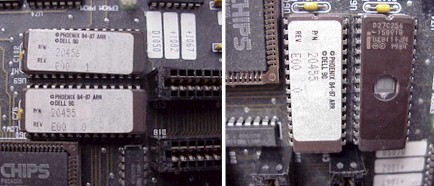
UV EPROMS - THE FIRST BIOS CHIPS

A UV EPROM (Ultraviolet Erasable) cannot be upgraded in the motherboard. The BIOS chip(s) must be removed, erased in an eprom eraser, and then reprogrammed with the updated code. Notice that there are two chips, this is because each chip is capable of delivering 8 bits of data. The early processors were 16 bits therefore you needed two 8 bit chips to deliver 16 bits in parallel. Also notice that on the label, in addition to the version information, there is a 0 and a 1. The 0 chip is the low order 8 bits and the 1 chip is the high order 8 bits. UV EPROM part numbers are 27 or 27C series (such as 27C256 or 27C512).
_______________________________________________________________________
FLASH EPROMS - 2ND GENERATION BIOS CHIPS
The first BIOS chips, UV EPROMs, were fabricated in packages with pins on two sides. These were called "Dual In-line" or "DIP" as there were two rows of pins on each side of the package. This same package was also used for FLASH EPROMs as they allow easy socketing of the parts. As motherboard manufacturers added additional features and interfaces, board space became a limiting factor. To gain space the BIOS DIP package was abandoned in favor of the smaller PLCC or "Plastic Leaded Chip Carrier". The PLCC package has pins on four sides and is about the size of a postage stamp. In some cases the PLCC BIOS is soldered directly to the motherboard which makes reprogramming a failed part extremely difficult. The photo on the right shows the same FLASH part (A290021) in both a DIP and PLCC package. These parts are exactly the same except for the package._______________________________________________________________________
FIRMWARE HUBS - THE 3RD GENERATION OF BIOS
As technology progressed, more functionality became concentrated in the motherboard chip set. The chip set provides the link between the processor and the hardware subsystems on the motherboard including the BIOS which was fabricated in a combination I/O and memory part called a FIRMWARE HUB. When the computer starts the chip set reads the BIOS data from the FIRMWARE HUB and loads it into system RAM. The processor then executes the BIOS code from RAM instead of from the part itself. This is different from how the original BIOS chips worked and has paved the way for the current versions of BIOS chips. FIRMWARE HUB parts were initially released by INTEL as they were the primary supplier of motherboard processors. FIRMWARE HUB parts are usually fabricated in 32 PIN PLCC packages._______________________________________________________________________
HIGH-SPEED SERIAL SPI FLASH EPROMS - TODAYS BIOS TECHNOLOGY
Modern motherboards, flat screen TVs, DVD players, home theatre receivers plus many other electronic products are now based on sophisticated, complex designs which start by booting from a BIOS chip. These products use the latest in high-speed, low cost memory technology parts called HI-SPEED SERIAL SPI FLASH EPROMs. SPI stands for "Serial Peripheral Interface". The SPI interface has existed for several decades but has now been incorporated into a flash eprom based high capacity part. The HI-SPEED SERIAL SPI FLASH EPROM is fabricated in either a DIP or surface mount 8 pin package. The SPI interface is serial (one bit at a time) which means that the data transfer speed must be extremely fast. As with a FIRMWARE HUB part, the SPI FLASH EPROMs function via the chip set to move the BIOS code from the part to system RAM for execution._______________________________________________________________________


No comments:
Post a Comment
Note: only a member of this blog may post a comment.